nz_lifer
Member
- Joined
- Aug 26, 2020
- Messages
- 87
Inspired by many sources.
One of the first videos I came across that piqued my interest was Brett's
Who happens to be a kiwi too, Bro 
Other videos of interest.
A big caveat, I am no electrical engineer.
The layout and track routing probably break all sorts of best practices.
My layman's assessment says it should work well enough.
Note you will need a microcontroller to drive this.
4x Outputs to drive the Analog Mux's.
1x Output per module. 64 channel would need 4x.
3x Output to drive the Shift Registers. Controls the charge/discharge function.
1x Input to sense charge completed.
2x ADC input for sensing Battery temperature and voltage.
There is a Red led for charging indicator.
Yellow for discharging.
Was going to flash them both to indicate the test cycle had completed.
I did not know about the Megacell project until I was already 90% done routing the board.
20+ hours in
Would I have still done this if I had found out sooner?
I think so.
https://www.indiegogo.com/projects/megacellcharger-mass-production#/
There are some interesting engineering choices they made.
Using the whole PCB as a heatsink? With sensors for monitoring battery temperature on the same PCB.
The software looks really good though, once debugged.
Discharge is not PWM, just straight on/off. Should not generate much switching interference.
Also means it is not constant current discharge.
But a function of the battery voltage.
The shift registers could be driven fast enough to simulate PWM.
The two data buses are the Shift Register and Analog Muxes.
Both are pretty low frequency and can be slowed down if interference starts to show up.
Any spikes should have minimal effect on the adc measurements.
I am using the ADS1115 16bit ADC to measure battery voltages.
Running at the 430 Samples/Second speed. PGA set to max voltage range 6.144.
Testing showed estimated mAh was within 1% when measured against a hobby battery charger, B6 clone.
This is without a current sense resistor, just accurate voltage measurement and calculating amperage using ohm's law. I=V/R
The fancy charger ramped down discharge current squeezing more mah out of them, iCharger 4010 Duo.
Shift registers over I/O Expanders for cost and expandability.
Although unless you go over 64 total cells, multiplexers would be fine.
For hobby use, costs are not a major either. Only matters if you are producing hundreds to sell.
Raw TP4056 IC over using completed modules.
The less soldering I have to do the better. If I am getting it populated might as well outsource as much as I can.
Switching the charging via a Mosfet rather than using the EN pin on the TP4056 IC.
This should give reverse battery protection too since it is now behind a Mosfet.
Temperature sensing, NTC Thermistor over a device like LM35.
Cost and availability. Not cheaply available locally here.
And I didn't know about it until the board was nearly completed.
I would have used them or something similar as they can be populated with the rest of the smd components.
Precision should be good enough for our purposes. These can go as accurate as 0.1c if processed right.
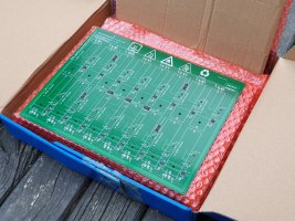
Board was sent for manufacturing on 25/08.
PCB manufacturing completed 28/08.
Component assembly completed 28/08.
Should be in my hands in 5 days.
Cost came to about us$18ea. Still unbelievably cheap compared to what was available not long ago.
Project is posted on EasyEDA
https://easyeda.com/recfvpernz/18650-chg-disc-rev1-web
There was a minimumorder of 5x boards.
If anyone wanted one and can help coding I can ship one to you.
I will do another post to give the R&D leading up this point.


One of the first videos I came across that piqued my interest was Brett's
Other videos of interest.
A big caveat, I am no electrical engineer.
The layout and track routing probably break all sorts of best practices.
My layman's assessment says it should work well enough.
Note you will need a microcontroller to drive this.
4x Outputs to drive the Analog Mux's.
1x Output per module. 64 channel would need 4x.
3x Output to drive the Shift Registers. Controls the charge/discharge function.
1x Input to sense charge completed.
2x ADC input for sensing Battery temperature and voltage.
There is a Red led for charging indicator.
Yellow for discharging.
Was going to flash them both to indicate the test cycle had completed.
I did not know about the Megacell project until I was already 90% done routing the board.
20+ hours in
Would I have still done this if I had found out sooner?
I think so.
https://www.indiegogo.com/projects/megacellcharger-mass-production#/
There are some interesting engineering choices they made.
Using the whole PCB as a heatsink? With sensors for monitoring battery temperature on the same PCB.
The software looks really good though, once debugged.
Discharge is not PWM, just straight on/off. Should not generate much switching interference.
Also means it is not constant current discharge.
But a function of the battery voltage.
The shift registers could be driven fast enough to simulate PWM.
The two data buses are the Shift Register and Analog Muxes.
Both are pretty low frequency and can be slowed down if interference starts to show up.
Any spikes should have minimal effect on the adc measurements.
I am using the ADS1115 16bit ADC to measure battery voltages.
Running at the 430 Samples/Second speed. PGA set to max voltage range 6.144.
Testing showed estimated mAh was within 1% when measured against a hobby battery charger, B6 clone.
This is without a current sense resistor, just accurate voltage measurement and calculating amperage using ohm's law. I=V/R
The fancy charger ramped down discharge current squeezing more mah out of them, iCharger 4010 Duo.
Shift registers over I/O Expanders for cost and expandability.
Although unless you go over 64 total cells, multiplexers would be fine.
For hobby use, costs are not a major either. Only matters if you are producing hundreds to sell.
Raw TP4056 IC over using completed modules.
The less soldering I have to do the better. If I am getting it populated might as well outsource as much as I can.
Switching the charging via a Mosfet rather than using the EN pin on the TP4056 IC.
This should give reverse battery protection too since it is now behind a Mosfet.
Temperature sensing, NTC Thermistor over a device like LM35.
Cost and availability. Not cheaply available locally here.
And I didn't know about it until the board was nearly completed.
I would have used them or something similar as they can be populated with the rest of the smd components.
Precision should be good enough for our purposes. These can go as accurate as 0.1c if processed right.
Board was sent for manufacturing on 25/08.
PCB manufacturing completed 28/08.
Component assembly completed 28/08.
Should be in my hands in 5 days.
Cost came to about us$18ea. Still unbelievably cheap compared to what was available not long ago.
Project is posted on EasyEDA
https://easyeda.com/recfvpernz/18650-chg-disc-rev1-web
There was a minimumorder of 5x boards.
If anyone wanted one and can help coding I can ship one to you.
I will do another post to give the R&D leading up this point.


Last edited:


